LNA
A bias-tee powered LNA
A wideband SPF5189Z low noise amplifier for an SDR, from schematic to a routed four layer layout, with FDTD, a cascade with vendor data, DC drop and thermal sims.
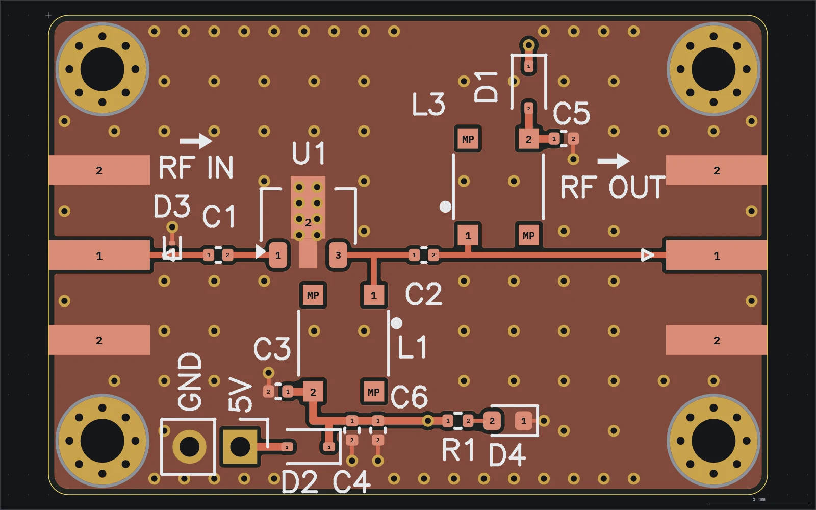
The amplifier sits at the antenna end of an RTL-SDR style receiver: SMA in, SMA out, a Qorvo SPF5189Z in the middle, powered either over the output coax by the receiver’s bias tee or from a 5 V header. Two Schottky diodes let either source power it without one feeding the other.
The RF lines are a field solved grounded coplanar class at 50 ohm on the top layer over the In1.Cu plane, with the pour beside it stitched to the plane every 2 mm. Its DESIGN.md records why each part was chosen, which chokes stay inductive up to 4 GHz, and the layout rules the circuit depends on.
The simulations show the usual split for RF work: an FDTD run of the passive board with a port where each active part sits, then a cascade that drops in the vendor .s2p files and the datasheet noise figure and OIP3. Change the board and rerun the FDTD; change a part and rerun only the cascade.
Open it
git clone https://github.com/v0l/agentee
cd agentee/examples/lna
agentee check
agentee view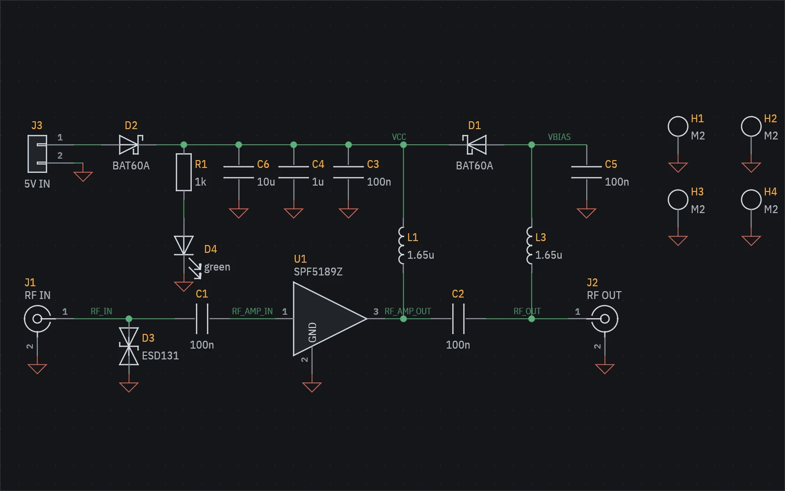
The LNA schematic: the input ESD clamp and DC block, the SPF5189Z, the bias chokes and the two power paths. 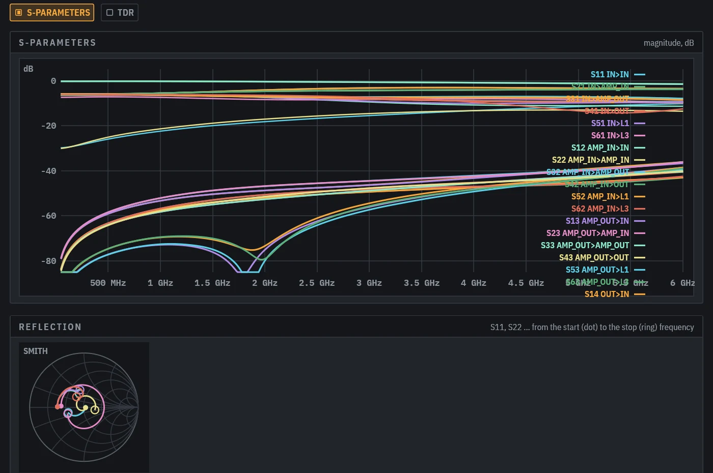
S-parameters of the LNA board from the FDTD run, with a Smith chart of the ports. 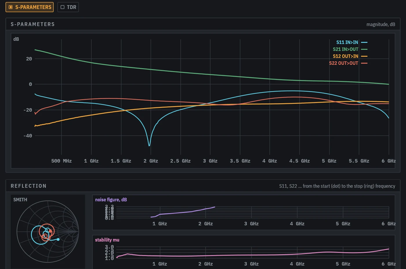
The cascade of the board with the SPF5189Z data: gain, match, noise figure and stability. 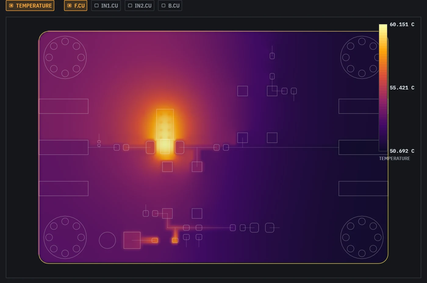
Thermal map of the LNA board with the amplifier as the hot spot. 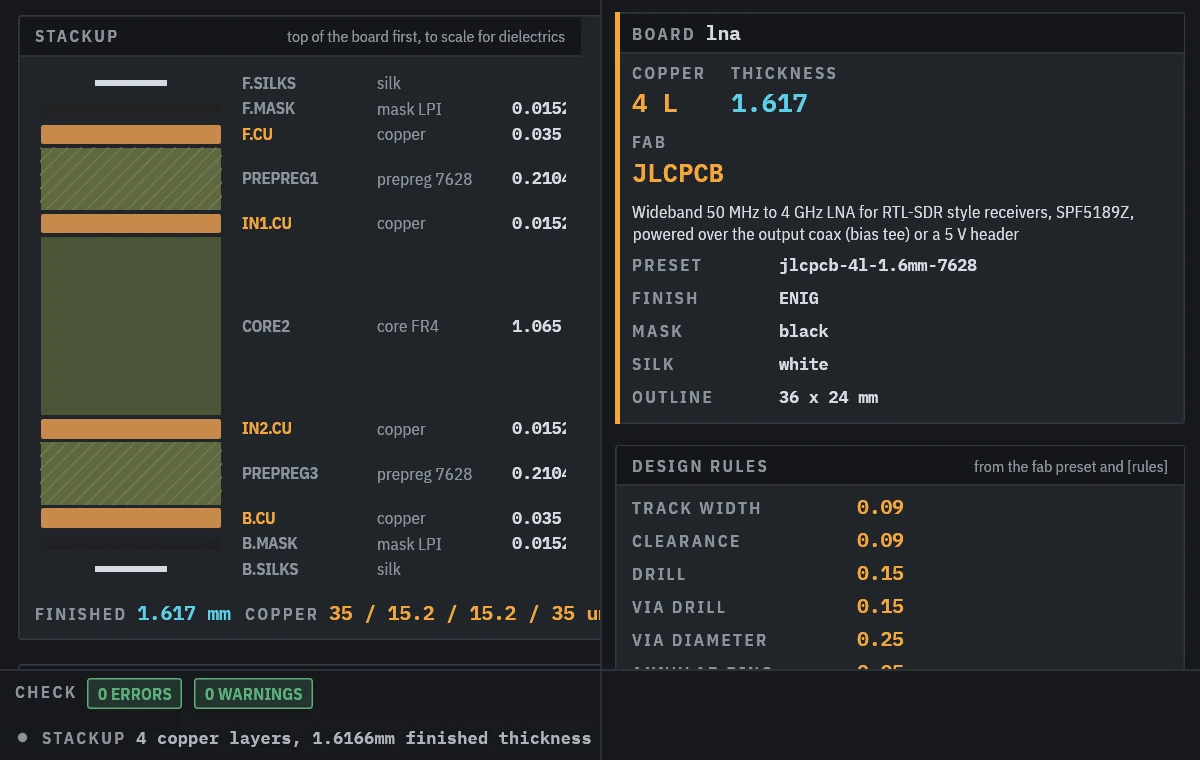
The LNA board spec: the four layer stackup to scale, the fab, finish and outline, and the design rules from the JLCPCB preset.