Start here
Your first board
From an empty directory to a checked, routed two layer board and a fab package: board spec, KiCad parts, a schematic, placement, routing and Gerbers.
This guide builds a small board by hand, one command at a time: a two pin power header, a resistor, a green LED and a decoupling capacitor on a two layer JLCPCB board. It is the same sequence an agent follows, so doing it once yourself makes it much easier to read what your agent is doing later.
You need agentee on your PATH and the KiCad libraries installed. See Install if you have neither.
Start a project
A project is a directory. Everything below it with a known suffix is loaded.
mkdir blinky && cd blinky
agentee new board blinky
agentee check
new board writes blinky.board.toml: a 50 by 30 mm outline, the JLCPCB two layer 1.6 mm stackup, one via type and four net classes. Check loads it and reports nothing:
0 sims, 0 layouts, 0 schematics, 1 boards, 0 symbols, 0 footprints: 0 errors, 0 warningscheck exits 0 when the project is clean, 1 when there are errors and 2 when a file does not load. That exit code is what lets an agent, or CI, loop on it.
Make the board the right size
Four parts do not need 50 by 30 mm. Shrink the outline:
agentee edit board blinky outline --size 30,18 --corner-radius 1mmagentee edit rewrites the TOML for you, keeps any comments in it, and runs check on the file it touched. Do not go much smaller on a board this simple: every board carries the agentee vX.Y.Z-HASH version in its silk, and check needs a clear strip about 23 by 1.2 mm to put it in. On a 20 mm board it reports a watermark error and the fab package is refused.
Import the parts
agentee reads the KiCad libraries rather than shipping its own. Search them, then import a symbol together with the footprint it should use:
agentee search symbol conn_01x02
agentee import symbol Connector_Generic:Conn_01x02 --footprint Connector_PinHeader_2.54mm:PinHeader_1x02_P2.54mm_Vertical
agentee import symbol Device:R --footprint Resistor_SMD:R_0603_1608Metric
agentee import symbol Device:LED --footprint LED_SMD:LED_0603_1608Metric
agentee import symbol Device:C --footprint Capacitor_SMD:C_0603_1608Metric
agentee check
Every word of a search must match the Library:Name. Imports land in symbols/ and footprints/ as TOML. Check now has something to say:
warning: ./footprints/R_0603_1608Metric.fp.toml: R_0603_1608Metric silk: silk lines under the fab minimum width 0.15mm: 2, thinnest 0.12mmKiCad draws silk at 0.12 mm and JLCPCB wants 0.15 mm. Open each footprint and change width = 0.12 to 0.15 on its silk graphics, or have your agent do it. This is the normal shape of work with agentee: the diagnostic names the file, the item and the number, and the fix is one edit.
Write the schematic
agentee new schematic blinkyThe starter is just a name. Add board = "blinky" under it, so the schematic knows which net classes exist. Then put the parts and nets in with one batch of commands, one per line:
agentee edit sch - <<'EOF'
add J1 Conn_01x02 PWR --footprint PinHeader_1x02_P2.54mm_Vertical
add R1 R 1k --footprint R_0603_1608Metric
add D1 LED green --footprint LED_0603_1608Metric
add C1 C 100n --footprint C_0603_1608Metric
net VIN J1.1 R1.1 C1.1 --class Power
net LED_A R1.2 D1.A --class Signal
net GND J1.2 D1.K C1.2 --class Ground --style power
EOF
A batch is one load and one check at the end, so the half-finished states in between are never flagged. Pins are REF.PIN, by number or by a unique pin name: D1.A is the anode, and the output confirms which number it resolved to.
added J1 (Conn_01x02)
added R1 (R)
added D1 (LED)
added C1 (C)
VIN now joins J1.1, R1.1, C1.1
LED_A now joins R1.2, D1.2
GND now joins J1.2, D1.1, C1.2
warning: /home/you/blinky/blinky.sch.toml: blinky part R1: body overlaps D1 (parts[2])
0 errors, 1 warnings in the files this touched
add puts each part to the right of the last, and the LED landed on the resistor. Move it, and the capacitor while you are there, then look:
agentee edit sch blinky move D1 25.4,0 --rotation 90
agentee edit sch blinky move C1 12.7,10.16
agentee render sch:blinky -o sch.png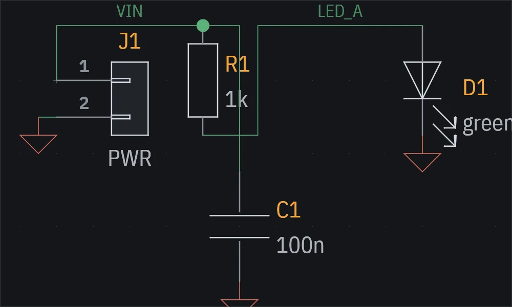
You did not draw a wire. A schematic lists nets as pins, and agentee routes the wires on the 1.27 mm grid when it draws them. Every net has a class; a net left in Default is a warning, because the class decides its track width, clearance and vias on the board.
Place the parts
agentee new layout blinkyAdd board = "blinky" and schematic = "blinky" to the starter. Check now fails, which is correct:
error: ./blinky.pcb.toml: blinky footprints: C1 is not placedPlace everything at once:
agentee place blinkyplace puts connectors on edges, keeps passives near what they connect to, refines the result and moves any reference label that now overlaps something. It prints a JSON report and writes at and rotation into a [[footprints]] entry per part. It is a quick start: on a real board you look at the result, move what matters by hand, mark it locked = true, and place the rest again.
Route it
Check now lists every connection that is missing:
error: ./blinky.pcb.toml: blinky net VIN: [unrouted] 2 unrouted: J1.1 | R1.1 | C1.1 are not joinedGive ground a pour on both layers, tie the ground pads to it, and route the other two nets:
agentee edit pcb blinky zone GND --layers F.Cu,B.Cu
agentee tie blinky
agentee route blinky --nets 'VIN,LED_A'
agentee check
tie puts a short stub and a via beside every SMD pad of a net that has a zone, which is how ground and supply pads should reach their plane. route routes the named nets on a grid, keeping each class's width and clearance, and appends ordinary [[tracks]] and [[vias]] to the layout. They are yours to edit afterwards.
0 sims, 1 layouts, 1 schematics, 1 boards, 4 symbols, 4 footprints: 0 errors, 0 warningsagentee render pcb:blinky -o pcb.png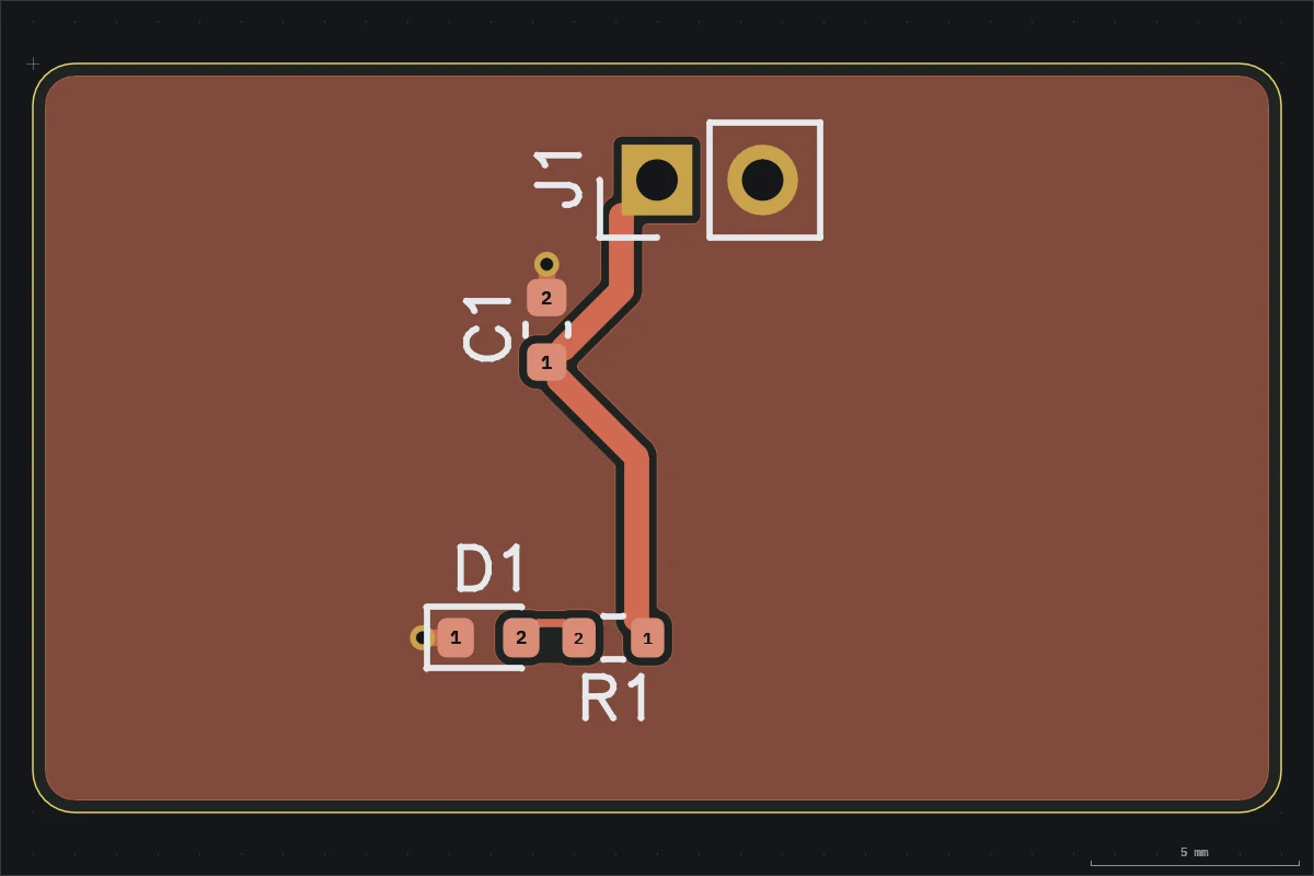
Write the fab package
agentee fab pcb:blinky -o fab/fab refuses while the layout has errors. With none, it writes the Gerbers for each layer, the drill file, a BOM and placement file in JLCPCB's columns, the IPC-D-356 netlist, assembly drawings, fab notes, and blinky-gerbers.zip to upload.
What you did
Every step was the same loop: one edit, check, look. Nothing kept state outside the files, so you can stop at any point, open the directory in git, or hand it to an agent with the skill and ask it to add a reverse polarity diode.
Next:
- Set up your coding agent so it can do all of this from a sentence.
- Board specs, stackups and net classes before a board where impedance or current matters.
agentee viewto watch the board update live while you or the agent edit it.